AI Weirdness: the strange side of machine learning

Tag: sem

Total 75 Posts
(Untitled)

(Untitled)

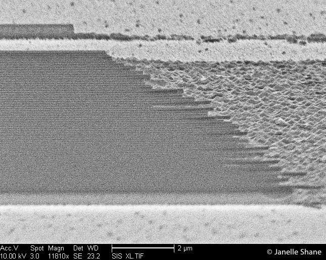
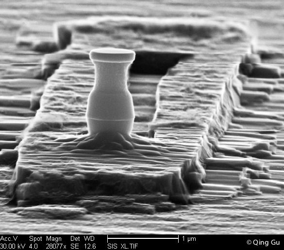
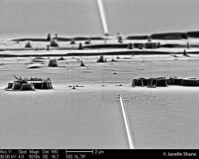
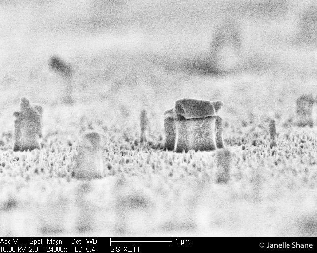
Top: An electron microscope photo of long, straight waveguides (left) interrupted by an accidental scratch during fabrication, that turned the orderly stripes into naturalistic chaos. Each structure is about 0.5 microns high, or less than 1/200 the thickness of a typical human hair. 
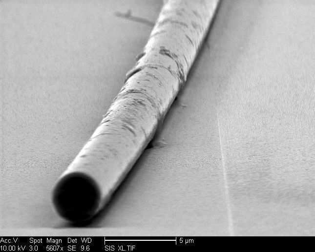
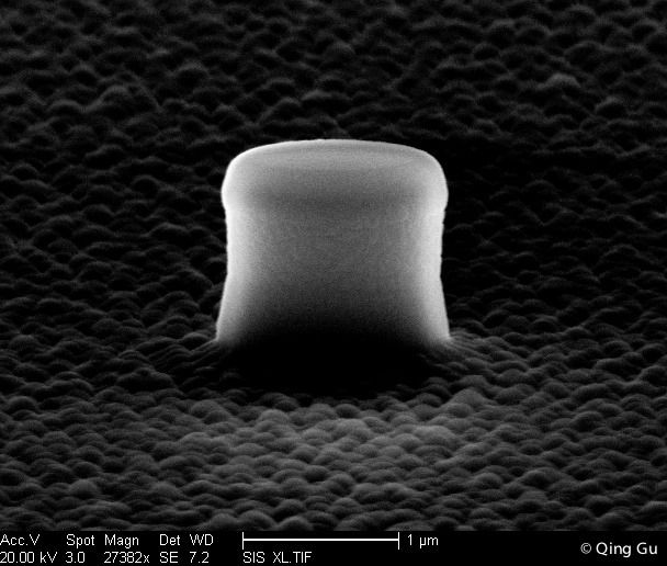
Bottom: A photo on quite
(Untitled)

(Untitled)

On the right: a photonic nanostructure, used in researching new light-based ways to make computers communicate faster. On the left: a single human hair (oops). Fortunately, according to Dr. Felipe Vallini of UCSD (who made and imaged this structure): “A hair hit my device, but he is still fine!”
(Untitled)

(Untitled)

A nano-lollipop?  This is a tiny glass ball on a tiny stick made of polymer, a partially-completed nano-sized chemical sensor made by then-grad-student Matthew Chen.  It’s on its way to becoming a nano-torch [http://lewisandquark.tumblr.com/post/92218390187/this-is-a-nanotorch-which-is-an-ultra-sensitive] , which can detect minute concentrations of chemicals due to
(Untitled)

(Untitled)

This is a nanotorch, which is an ultra-sensitive chemical detector, thanks to its ability to concentrate light.  In the intense light fields at the torch’s top, a normally-weak light-based chemical fingerprinting technique (Raman spectroscopy) becomes millions of times stronger.  More-sensitive Raman fingerprinting can allow us to detect trace contaminants
(Untitled)

(Untitled)

When a nanolaser casts a shadow, the grad student gets 6 more weeks of fabrication. The pillar in the middle is one of the nanolasers our lab makes.  It’s supposed to be a single column all by itself, roughly cylindrical with a bit of a funky coke bottle shape,
(Untitled)

(Untitled)

Oops.  When we’re making nano-devices, chaos is usually bad.  I named this spot “The Barrens”. It’s supposed to be a single straight waveguide (basically, a pipe for light) stretching off into infinity.  Instead, this spot got scratched partway through the fabrication process, leaving behind a chaotic landscape that
(Untitled)

(Untitled)

The cliffs of insanity?  Rising an awe-inspiring 1.5 microns above the wave-lashed sea (about 1/100 the thickness of a sheet of printer paper), these cliffs were formed when high-energy plasma ate away a layer of semiconductor.  All that was left behind was this island, protected by a glassy
(Untitled)

(Untitled)

Like a tiny shiny mountain, this nanolaser and the area around it is coated in a layer of blobby silver.  The silver serves as a mirror that keeps the laser light bouncing around inside the laser’s light-amplifying interior, generating more and more copies of itself.  A tiny percentage of
(Untitled)

(Untitled)

A nanoscale landscape, peopled with little pillars.  Each of these would fit easily inside a single cell.  They were created out of semiconductor (the same sort that can be made into lasers), when a high-energy plasma ate away everything that wasn’t protected. Each little pillar has a cap on
(Untitled)

(Untitled)

A Devil’s Tower-like monument rises above a sea of bubbles.  It’s just another day in the life of a nanolaser researcher. The tower is a microscopic laser in the process of being built - here, it’s shown after it was carved out of a flat sheet of
You've successfully subscribed to AI Weirdness
Great! Next, complete checkout for full access to AI Weirdness
Welcome back! You've successfully signed in.
Unable to sign you in. Please try again.
Success! Your account is fully activated, you now have access to all content.
Error! Stripe checkout failed.
Success! Your billing info is updated.
Error! Billing info update failed.