

(Untitled)
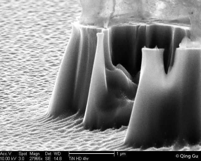
The cliffs of insanity? Rising an awe-inspiring 1.5 microns above the wave-lashed sea (about 1/100 the thickness of a sheet of printer paper), these cliffs were formed when high-energy plasma ate away a layer of semiconductor. All that was left behind was this island, protected by a glassy layer of photoresist. The photoresist didn’t weather the effects of the plasma very well; you can see how it was shredded by the blast of plasma, making the edges of the cliffs naturalistically random. We use the combination of plasma etcher and protective resist to make nanoscale devices, like tiny lasers and filters and switches.
Fabrication and scanning electron microscope image by my labmate Dr. Qing Gu.
Subscribe now
Already have an account? Sign in