AI Weirdness: the strange side of machine learning

Tag: nanolandscape

Total 30 Posts
(Untitled)

(Untitled)

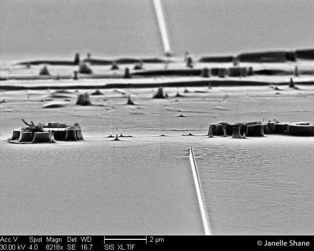
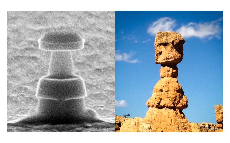
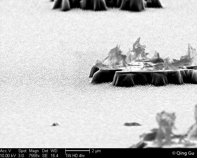
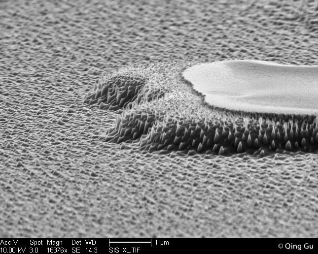
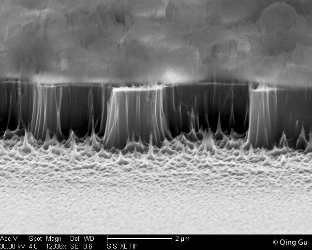
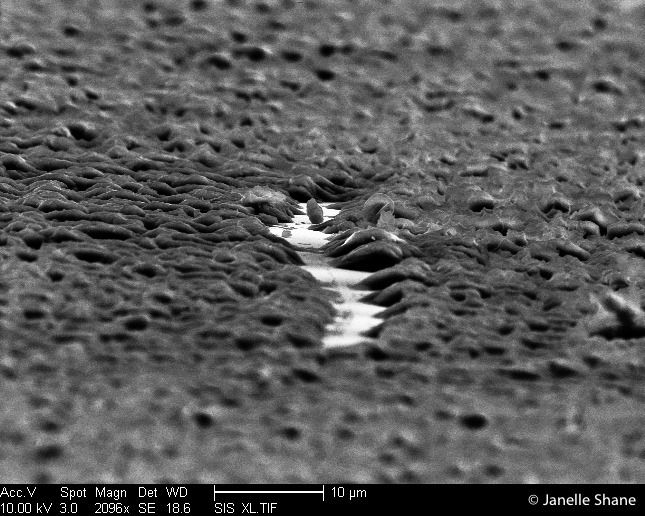
Oops.  When we’re making nano-devices, chaos is usually bad.  I named this spot “The Barrens”. 
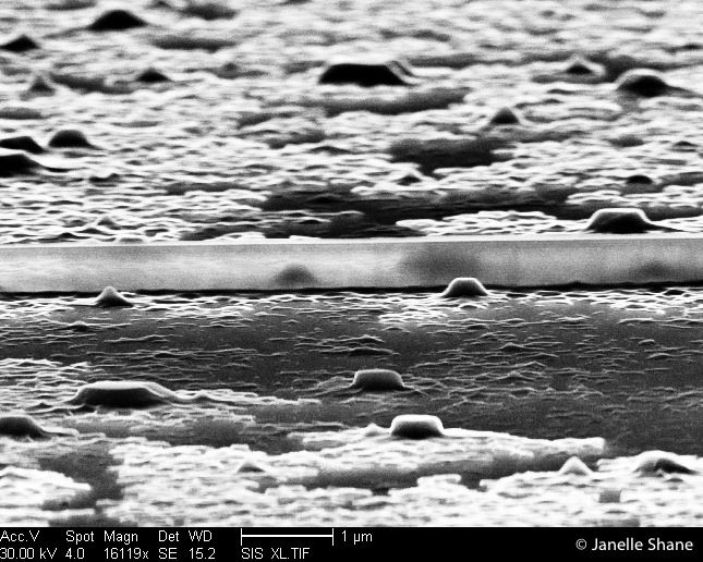
It’s supposed to be a single straight waveguide (basically, a pipe for light) stretching off into infinity.  Instead, this spot got scratched partway through the fabrication process, leaving behind a chaotic landscape that
(Untitled)

(Untitled)

The cliffs of insanity?  Rising an awe-inspiring 1.5 microns above the wave-lashed sea (about 1/100 the thickness of a sheet of printer paper), these cliffs were formed when high-energy plasma ate away a layer of semiconductor.  All that was left behind was this island, protected by a glassy
(Untitled)

(Untitled)

A strange landscape with an even stranger sky. This is a microscope view of the edge of a smooth chunk of silicon, coated with a thin clear plasticy layer of photoresist.  Just like the colors in a soap bubble, this colorless thin layer produces rainbow colors due to the wave
(Untitled)

(Untitled)

A Devil’s Tower-like monument rises above a sea of bubbles.  It’s just another day in the life of a nanolaser researcher. The tower is a microscopic laser in the process of being built - here, it’s shown after it was carved out of a flat sheet of
(Untitled)

(Untitled)

The one on the left is a nanolaser, carved by high-energy plasma and strong acid, and invisible to the naked eye.  The one on the right is a hoodoo, carved by wind and rain, and is approximately 20 million times larger. And about 60 million times older. The reason they
(Untitled)

(Untitled)

It looks like it could be an image of desert badlands - except for that strangely translucent wall.  In fact, this scene is much, much smaller. An ant could step over the wall without ever noticing its existence. This image was taken through an electron microscope, of a microscopic landscape
(Untitled)

(Untitled)

Resembling arrays of flaming islands, these formations are actually microscopic, etched out of semiconductor. This semiconductor material is what we use to make microscopic lasers - we start with a vast, featureless sheet of semiconductor and cover certain areas with a protective layer of glassy photoresist.  Then we blast the
(Untitled)

(Untitled)

Strange formations caused when high-energy plasma from a reactive ion etcher bombards semiconductor materials. We use the reactive ion etcher to carve out microscopic optical devices, like lasers and filters.  Here, there’s no particular device that we were trying to make - we were just testing to see if
(Untitled)

(Untitled)

The cliffs of fluffiness!  Lashed by impossibly pointy nano-waves. The fluffy stuff at the top is actually photoresist, a glassy substance that we use to protect semiconductor from plasma bombardment when we’re doing our etching.  Here, the photoresist protected the semiconductor below it from being etched away, making the
(Untitled)

(Untitled)

The long valley, surrounded by jagged mountains, occupied by a picturesque leaning castle….  Actually, this is a closeup of a minuscule scratch in a coating of photoresist.  At this magnification (2096x), it’s clear that the photoresist has a rough, mountainous surface, caused by the high-energy plasma I’d bombarded
You've successfully subscribed to AI Weirdness
Great! Next, complete checkout for full access to AI Weirdness
Welcome back! You've successfully signed in.
Unable to sign you in. Please try again.
Success! Your account is fully activated, you now have access to all content.
Error! Stripe checkout failed.
Success! Your billing info is updated.
Error! Billing info update failed.