AI Weirdness: the strange side of machine learning

Tag: nanocliff

Total 10 Posts
(Untitled)

(Untitled)

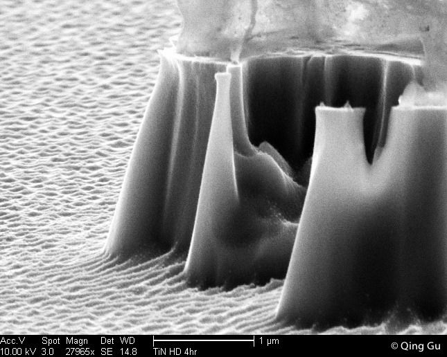
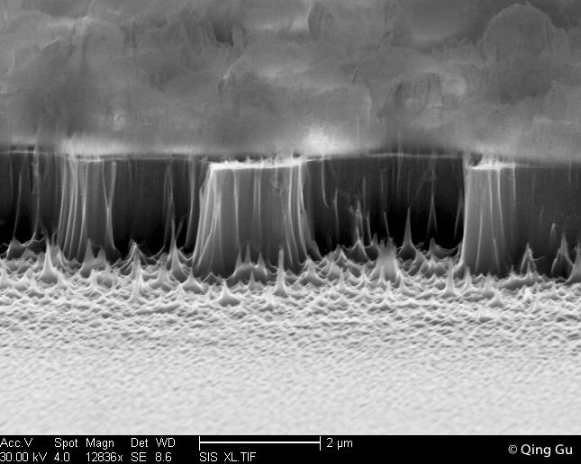
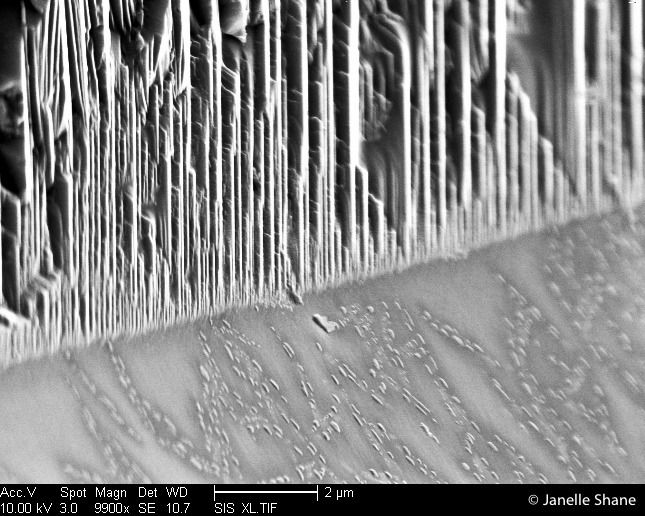
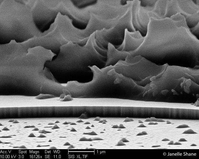
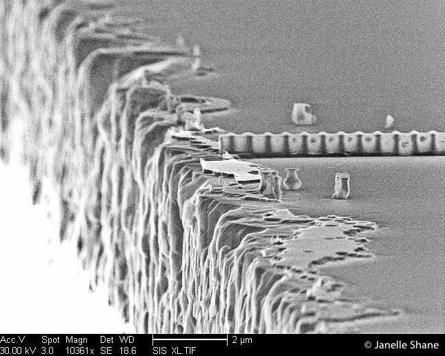
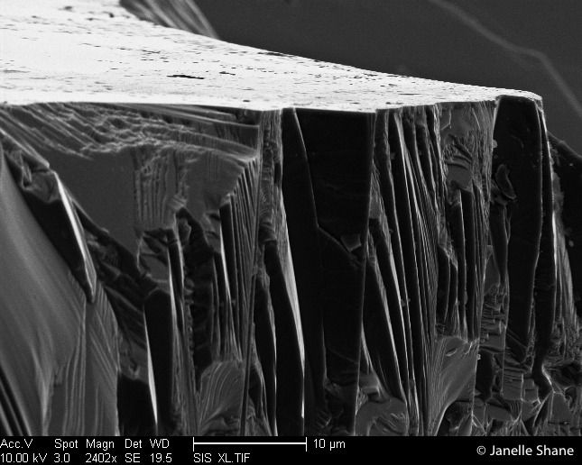
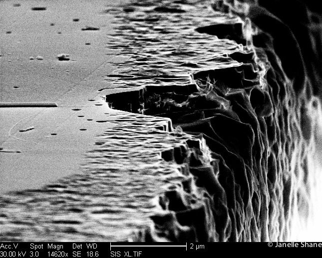
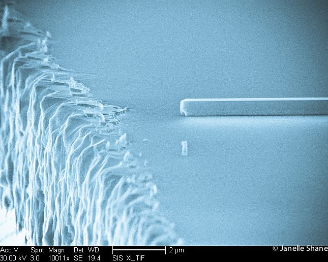
The cliffs of insanity?  Rising an awe-inspiring 1.5 microns above the wave-lashed sea (about 1/100 the thickness of a sheet of printer paper), these cliffs were formed when high-energy plasma ate away a layer of semiconductor.  All that was left behind was this island, protected by a glassy
(Untitled)

(Untitled)

The cliffs of fluffiness!  Lashed by impossibly pointy nano-waves. The fluffy stuff at the top is actually photoresist, a glassy substance that we use to protect semiconductor from plasma bombardment when we’re doing our etching.  Here, the photoresist protected the semiconductor below it from being etched away, making the
(Untitled)

(Untitled)

The microscopic fractured edge of a piece of semiconductor looms like an enormous cliff face.  However, this entire view would fit easily inside the diameter of a single human hair.  At the top of the cliff is a rough dark layer, the remains of a protective layer that we bombarded
(Untitled)

(Untitled)

Fracture patterns at the edge of a broken wafer (broken on purpose, for once).  The lighter top layer is silicon, and the darker bottom layer is glass.  The glass looks darker than the silicon because it’s a better electrical insulator - the electron beam microscope makes an image by
(Untitled)

(Untitled)

Microscopic fracture patterns appear clifflike on the edge of one of my samples.  This entire view is less than 10 micrometers high, meaning that it covers about a tenth the thickness of a typical human hair.  We usually don’t get patterns like these, because we use a special wafer
(Untitled)

(Untitled)

The crazy-huge mountains of the nanoworld!  The strange waves and scallops are what is left of the protective mask I used to shield the semiconductor material below from a high-energy etching plasma.  The mask held up to the plasma, although it was probably damaged a bit - and then I
(Untitled)

(Untitled)

Standing at the edge of the world. At microscopic scales, even a clean break isn’t very clean - this electron microscope picture is of the edge of a piece of glass, on which I had fabricated a long wall of semiconductor (the long columned wall you see at the
(Untitled)

(Untitled)

The broken edge of a piece of semiconductor laser material, viewed at 2,402x under an electron microscope.  At this magnification, it’s clear that the edge isn’t cleanly broken at all, but has all sorts of furrows and ripples, all invisible to the naked eye, making it look
(Untitled)

(Untitled)

Here’s another view of the sample I posted earlier, the one that was so wonderfully, spectacularly ruined. This time I’ve zoomed in near the very edge of the chip, where the vast plain of laser material abruptly ends at a jagged cliff.  By the time I was looking
(Untitled)

(Untitled)

It’s a serene sight - a nicely formed wall of laser material (semiconductor InGaAsP, to be exact) stands on a smooth glassy plain. I added the color - it’s not actually cold here.  It’s inhospitable in a different sense, though: There isn’t any air.  For the
You've successfully subscribed to AI Weirdness
Great! Next, complete checkout for full access to AI Weirdness
Welcome back! You've successfully signed in.
Unable to sign you in. Please try again.
Success! Your account is fully activated, you now have access to all content.
Error! Stripe checkout failed.
Success! Your billing info is updated.
Error! Billing info update failed.