

Monday November 18, 2013
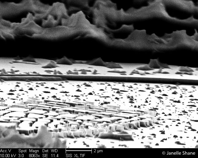
This image is from a test of our plasma etcher, and shows a white plain of semiconductor laser material etched partially away by plasma. In the background is the black remains of photoresist that was protecting other areas of semiconductor from being etched - it did the job, but took some damage, sculpted into jagged mountains by the plasma. We have to take this effect into consideration when we want to etch deep into semiconductor - we need to make sure that the protective photoresist is thick enough to withstand the plasma blast.
In this case, the test was a success - we only wanted to make sure that the plasma etching was working at all. By the cool network of broken canyons in the foreground, we can definitely tell that the plasma was doing its job.